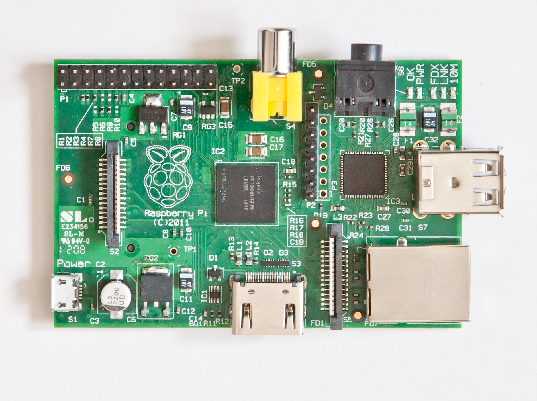
Right now the bare FR4 substrate is drawn in the same color as the
soldermask so trying to see details of soldermask cutouts (for example,
when designing a fiducial or PCB antenna that needs mask clearance
around it) is difficult. Does anyone else find this hard to see?
It should probably be displayed in some kind of yellow/tan/brown color
as that's what actual un-masked FR4 looks like (for example, around the
fiducials in
http://upload.wikimedia.org/wikipedia/commons/9/90/Front_of_Raspberry_Pi.jpg)

--
Andrew Zonenberg
PhD student, security group
Computer Science Department
Rensselaer Polytechnic Institute
http://colossus.cs.rpi.edu/~azonenberg/
![]() signature.asc
signature.asc
Description: This is a digitally signed message part
_______________________________________________
Mailing list: https://launchpad.net/~kicad-developers
Post to     : kicad-developers@lists.launchpad.net
Unsubscribe : https://launchpad.net/~kicad-developers
More help   : https://help.launchpad.net/ListHelp