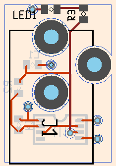
In case anyone wants to provide feedback about the third "first
board", here are my notes and sample board so far.  Yes, a four layer
board is overkill, and I'm intentionally shrinking the board more than
is needed.  This is a tutorial, not something practical :-)
http://www.delorie.com/pcb/gs-smt.png

Third board: 555 blinky light again, same schematic.  SMT, four layer,
internal power planes.  New: SMT, layers, vias, thermals, polygon
planes.

Same basic schematic
name GND and VDD nets

gattrib:
MSOP8   LMC555CMM Nat Semi
0603's

PCB:
50mm x 50mm
8/8 rules, 15 mil drill vias
4 layers: component, gnd, power, solder

gsch2pcb as usual

move parts to solder side
position under power jack
move to upper left, shrink to 12.5 x 18mm board

rectangle tool - gnd plane
poly tool - power plane
thermals

via tool - vias near power/gnd connections, manually route

autoroute remainder


_______________________________________________
geda-user mailing list
[email protected]
http://www.seul.org/cgi-bin/mailman/listinfo/geda-user